Sense amplifier
In modern computer memory, a sense amplifier is one of the elements which make up the circuitry on a semiconductor memory chip (integrated circuit); the term itself dates back to the era of magnetic core memory.[1] A sense amplifier is part of the read circuitry that is used when data is read from the memory; its role is to sense the low power signals from a bitline that represents a data bit (1 or 0) stored in a memory cell, and amplify the small voltage swing to recognizable logic levels so the data can be interpreted properly by logic outside the memory.[2]
Modern sense-amplifier circuits consist of two to six (usually four) transistors, while early sense amplifiers for core memory sometimes contained as many as 13 transistors.[3] There is one sense amplifier for each column of memory cells, so there are usually hundreds or thousands of identical sense amplifiers on a modern memory chip. As such, sense amplifiers are one of the only analog circuits in a computer's memory subsystem.
Basic structure

Sense amplifier is required during the data read and refresh operation from the memory concerned.
| Circuit Types | Operation Mode |
|---|---|
| Differential | Voltage-mode |
| Nondifferential | Current-mode |
Memory chip operation
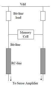
The data in a semiconductor memory chip is stored in tiny circuits called memory cells. Sense Amplifiers are primarily applied in Volatile memory cells. The memory cells are either SRAM or DRAM cells which are laid out in rows and columns on the chip. Each line is attached to each cell in the row. The lines which run along the rows are called wordlines which are activated by putting a voltage on it. The lines which run along the columns are called bit-line and two such complementary bitlines are attached to a sense amplifier at the edge of the array. Number of sense amplifiers are of that of the "bitline' on the chip. Each cell lies at the intersection of a particular wordline and bitline, which can be used to "address" it. The data in the cells is read or written by the same bit-lines which run along the top of the rows and columns.[4]
SRAM operation
To read a bit from a particular memory cell, the wordline along the cell's row is turned on, activating all the cells in the row. The stored value (Logic 0 or 1) from the cell then comes to the Bit-lines associated with it. The sense amplifier at the end of the two complimentary bit-lines amplify the small voltages to a normal logic level. The bit from the desired cell is then latched from the cell's sense amplifier into a buffer, and put on the output bus.[5]
DRAM operation
The sense amplifier operation in DRAM is quite similar to the SRAM, but it performs an additional function. The data in DRAM chips is stored as electric charge in tiny capacitors in the memory cells. The read operation depletes the charge in a cell, destroying the data, so after the data is read out the sense amplifier must immediately write it back in the cell by applying a voltage to it, recharging the capacitor. This is called memory refresh.
Design objectives
As part of their designs, sense amplifiers aim at a minimum sense delay, required level of amplification, minimum power consumption, fit into restricted layout areas, and high reliability and tolerance.
See also
References
- ↑ PDP-8 Maintenance Manual, Digital Equipment Corporation, F-87, 2/66, 1966; pages 4-1 to 4-13.
- ↑ A Low-Power SRAM Using Bit-Line Charge-Recycling for Read and Write Operations, IEEE Journal of Solid-State Circuits, 2010 IEEE
- ↑ PDP-8 Maintenance Manual, Digital Equipment Corporation, F-87, 2/66, 1966; page 10-9 drawing RS-B-G007.
- ↑ Characterization of SRAM sense amplifier input offset for yield prediction in 28nm CMOS, Custom Integrated Circuits Conference (CICC), 2011 IEEE
- ↑ Sense Amplifier for SRAM , Prof: Der-Chen Huang, National Chung Hsing University