PIN diode

A PIN diode is a diode with a wide, undoped intrinsic semiconductor region between a p-type semiconductor and an n-type semiconductor region. The p-type and n-type regions are typically heavily doped because they are used for ohmic contacts.
The wide intrinsic region is in contrast to an ordinary p–n diode. The wide intrinsic region makes the PIN diode an inferior rectifier (one typical function of a diode), but it makes it suitable for attenuators, fast switches, photodetectors, and high voltage power electronics applications.
Operation
A PIN diode operates under what is known as high-level injection. In other words, the intrinsic "i" region is flooded with charge carriers from the "p" and "n" regions. Its function can be likened to filling up a water bucket with a hole on the side. Once the water reaches the hole's level it will begin to pour out. Similarly, the diode will conduct current once the flooded electrons and holes reach an equilibrium point, where the number of electrons is equal to the number of holes in the intrinsic region. When the diode is forward biased, the injected carrier concentration is typically several orders of magnitude higher than the intrinsic carrier concentration. Due to this high level injection, which in turn is due to the depletion process, the electric field extends deeply (almost the entire length) into the region. This electric field helps in speeding up of the transport of charge carriers from the P to the N region, which results in faster operation of the diode, making it a suitable device for high frequency operations.
Characteristics
A PIN diode obeys the standard diode equation for low frequency signals. At higher frequencies, the diode looks like an almost perfect (very linear, even for large signals) resistor. There is a lot of stored charge in the intrinsic region. At low frequencies, the charge can be removed and the diode turns off. At higher frequencies, there is not enough time to remove the charge, so the diode never turns off. The PIN diode has a poor reverse recovery time.
The high-frequency resistance is inversely proportional to the DC bias current through the diode. A PIN diode, suitably biased, therefore acts as a variable resistor. This high-frequency resistance may vary over a wide range (from 0.1 Ω to 10 kΩ in some cases;[1] the useful range is smaller, though).
The wide intrinsic region also means the diode will have a low capacitance when reverse-biased.
In a PIN diode, the depletion region exists almost completely within the intrinsic region. This depletion region is much larger than in a PN diode, and almost constant-size, independent of the reverse bias applied to the diode. This increases the volume where electron-hole pairs can be generated by an incident photon. Some photodetector devices, such as PIN photodiodes and phototransistors (in which the base-collector junction is a PIN diode), use a PIN junction in their construction.
The diode design has some design trade-offs. Increasing the dimensions of the intrinsic region (and its stored charge) allows the diode to look like a resistor at lower frequencies. It adversely affects the time needed to turn off the diode and its shunt capacitance. It is therefore necessary to select a device with the appropriate properties for a particular use.
Applications
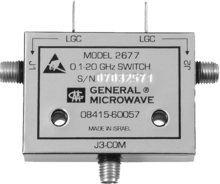
PIN diodes are useful as RF switches, attenuators, photodetectors, and phase shifters.[2]
RF and microwave switches

Under zero- or reverse-bias (the "off" state), a PIN diode has a low capacitance. The low capacitance will not pass much of an RF signal. Under a forward bias of 1 mA (the "on" state), a typical PIN diode will have an RF resistance of about 1 ohm, making it a good RF conductor. Consequently, the PIN diode makes a good RF switch.
Although RF relays can be used as switches, they switch very slowly (on the order of 10 milliseconds). A PIN diode switch can switch much more quickly (e.g., 1 microsecond).
For example, the capacitance of an "off"-state discrete PIN diode might be 1 pF. At 320 MHz, the capacitive reactance of 1 pF is 497 ohms:
As a series element in a 50 ohm system, the off-state attenuation in dB is:
This attenuation may not be adequate. In applications where higher isolation is needed, both shunt and series elements may be used, with the shunt diodes biased in complementary fashion to the series elements. Adding shunt elements effectively reduces the source and load impedances, reducing the impedance ratio and increasing the off-state attenuation. However, in addition to the added complexity, the on-state attenuation is increased due to the series resistance of the on-state blocking element and the capacitance of the off-state shunt elements.
PIN diode switches are used not only for signal selection, but also component selection. For example, some low phase noise oscillators use them to range-switch inductors.[3]
RF and microwave variable attenuators

By changing the bias current through a PIN diode, it is possible to quickly change the RF resistance.
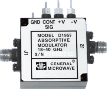
At high frequencies, the PIN diode appears as a resistor whose resistance is an inverse function of its forward current. Consequently, PIN diode can be used in some variable attenuator designs as amplitude modulators or output leveling circuits.
PIN diodes might be used, for example, as the bridge and shunt resistors in a bridged-T attenuator. Another common approach is to use PIN diodes as terminations connected to the 0 degree and -90 degree ports of a quadrature hybrid. The signal to be attenuated is applied to the input port, and the attenuated result is taken from the isolation port. The advantages of this approach over the bridged-T and pi approaches are (1) complementary PIN diode bias drives are not needed—the same bias is applied to both diodes—and (2) the loss in the attenuator equals the return loss of the terminations, which can be varied over a very wide range.
Limiters
PIN diodes are sometimes used as input protection devices for high frequency test probes. If the input signal is within range, the PIN diode has little impact as a small capacitance. If the signal is large, then the PIN diode starts to conduct and becomes a resistor that shunts most of the signal to ground.
Photodetector and photovoltaic cell
The PIN photodiode was invented by Jun-ichi Nishizawa and his colleagues in 1950.
PIN photodiodes are used in fibre optic network cards and switches. As a photodetector, the PIN diode is reverse-biased. Under reverse bias, the diode ordinarily does not conduct (save a small dark current or Is leakage). When a photon of sufficient energy enters the depletion region of the diode, it creates an electron, hole pair. The reverse bias field sweeps the carriers out of the region creating a current. Some detectors can use avalanche multiplication.
The same mechanism applies to the PIN structure, or p-i-n junction, of a solar cell. In this case, the advantage of using a PIN structure over conventional semiconductor p–n junction is the better long wavelength response of the former. In case of long wavelength irradiation, photons penetrate deep into the cell. But only those electron-hole pairs generated in and near the depletion region contribute to current generation. The depletion region of a PIN structure extends across the intrinsic region, deep into the device. This wider depletion width enables electron-hole pair generation deep within the device. This increases the quantum efficiency of the cell.
Commercially available PIN photodiodes have quantum efficiencies above 80-90% in the telecom wavelength range (~1500 nm), and are typically made of germanium or InGaAs. They feature fast response times (higher than their p-n counterparts), running into several tens of gigahertz,[4] making them ideal for high speed optical telecommunication applications. Similarly, silicon p-i-n photodiodes[5] have even higher quantum efficiencies, but can only detect wavelengths below the bandgap of silicon, i.e. ~1100 nm.
Typically, amorphous silicon thin-film cells use PIN structures. On the other hand, CdTe cells use NIP structure, a variation of the PIN structure. In a NIP structure, an intrinsic CdTe layer is sandwiched by n-doped CdS and p-doped ZnTe. The photons are incident on the n-doped layer unlike a PIN diode.
A PIN photodiode can also detect X-ray and gamma ray photons.
Example diodes
SFH203 and BPW43 are cheap general purpose PIN diodes in 5 mm clear plastic cases with bandwidths over 100 MHz. RONJA telecommunication systems are an example application.
See also
- Step recovery diode
- Optical interconnect
- Light Peak
- Interconnect bottleneck
- Optical fiber cable
- Optical communication
- Parallel optical interface
References
- ↑ Doherty, Bill, MicroNotes: PIN Diode Fundamentals (PDF), Watertown, MA: Microsemi Corp., MicroNote Series 701 (undated)
- ↑ http://srmsc.org/pdf/004430p0.pdf (transcript version: http://www.alternatewars.com/WW3/WW3_Documents/ABM_Bell/ABM_Ch8.htm)
- ↑ About RF Switches – Herley General Microwave
- ↑ "Discovery semiconductor 40G InGaAs photodetector modules".
- ↑ "Si photodiodes | Hamamatsu Photonics". www.hamamatsu.com. Retrieved 2015-09-27.