Ian A. Young
| Ian A. Young | |
|---|---|
 | |
| Born | Melbourne, Victoria |
| Residence | Portland, Oregon |
| Citizenship | United States, Australia |
| Fields | X86, Microprocessors, Phase-locked loop, Clock signal, Mixed-signal integrated circuit, Photonics, Spintronics, Dynamic random-access memory, Static random-access memory, Switched capacitor, Analog-to-digital converter |
| Institutions | Intel, University of California, Berkeley, Mostek |
| Alma mater | University of California, Berkeley, University of Melbourne, Australia |
| Thesis | MOS switched-capacitor analog sampled-data recursive filters (1978) |
| Doctoral advisor | David A. Hodges, Paul R. Gray |
| Known for | Intel Microprocessor Clock Scaling from 50 MHz to 3 GHz, Analog MOS Circuits, Phase-locked loop |
| Influences | Semiconductor Research Corporation DARPA IEEE |
| Notable awards | Fellow, IEEE 1999; Intel Achievement Awards (3 times), Fellow Intel 1996, Senior Fellow Intel 2004 |
Ian. A. Young is an Intel Senior Fellow [1] and Director at Intel Corporation, leading the research in beyond CMOS. Young is a co-inventor of the original design for Intel microprocessor clocking that led to the successful Moore's law scaling of Intel Pentium (brand) and Intel Core processors from 50 MHz to 3 GHz.[2] PLL is the most shipped analog circuit in integrated circuit chips.[3]
Young was a primary inventor on Intel BiCMOS logic circuit family,[4][5] adopted in Pentium, Pentium Pro, Pentium II microprocessors. Young also developed microprocessor performance optimization metric for transistors (Front End Transistor Metric) and interconnects,[6] which have been in continuous use since 250 nanometer semiconductor technology node. He helped lay the groundwork for today’s fully integrated PCIe and Intel Quick Path Interconnect (QPI) chip-to-chip I/O.
Young has written 50 [7] research papers and 71 patents[8] in switched capacitor circuits, DRAM, SRAM, BiCMOS, x86 clocking, Photonics and spintronics.
Biography
Born in Melbourne, Australia, Young received his bachelor's and master's degrees in electrical engineering from the University of Melbourne, Australia. He received his Ph.D. in electrical engineering from the University of California, Berkeley in 1978, where he did pioneering research on MOSFET switched-capacitor filters.[9] Prior to Intel, he worked on analog/digital integrated circuits for telecommunications products at Mostek Corporation.
Technical career
Early Career, Analog MOS Integrated Circuits & Switched Capacitor Filters
Young obtained his PhD from University of California, Berkeley in 1978 working with David A. Hodges developing the first switched MOS capacitor circuits which later developed into analog MOS switched capacitor filters.[9][10] In 1977, Young (then a Ph.D. student) with David A. Hodges and Paul Gray (at Berkeley) demonstrated an All-MOS sampled-data second-order active filter using a precise clock reference, four operational amplifiers, analog switches and ratioed capacitors all fabricated on an NMOS integrated circuit.[11]
Intel BiCMOS for Logic & SRAM
Young started at Intel in 1983 with the development of circuits for the world’s first 1 Mb DRAM in 1 μm CMOS in 1985,[12] and first 64 K SRAM in 1 μm CMOS. This was also the first military qualified SRAM under the VHIC program.[13] He then led the design of 800 nanometer, 600 nanometer, 350 nanometer SRAM products and manufacturing test vehicles. At 600 nanometer node, Intel adopted BiCMOS for logic requiring the development of a BiCMOS SRAM for cache and a new family of standard logic circuits.
The BiCMOS logic family employed the npn devices in the pull-up path of the BiCMOS gate, to form a low power CMOS logic family with high capacitive drive capability. Intel's BiCMOS technology was enabled by an innovative triple diffused npn transistor. This led to a highly manufacturable low cost process due to minimum number of additional process steps. In contrast, other companies employed BiCMOS to implement Emitter-coupled logic for microprocessors, which consumed much more power. The BiCMOS circuits were developed for the Pentium processor family and its follow-on generations Pentium Pro, Pentium II processor family.
Pentium Era and Clock Scaling
Young developed the original Phase Locked Loop (PLL) based clocking circuit in a microprocessor while working on the 50 MHz Intel 80486 processor design. He subsequently developed the core PLL clocking circuit building blocks used in each generation of Intel microprocessors through the 0.13 μm 3.2 GHz Pentium 4. The successful introduction of GHz clocking contributed to massive improvements in computing power.

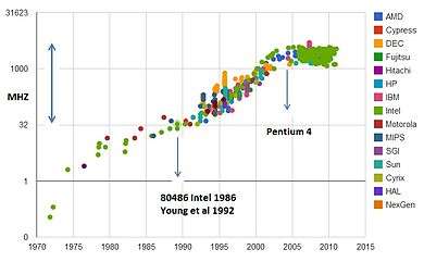
The Clock rate scaling ushered by Intel and AMD ended as the thermal power dissipation of processors reached 100 W/cm^2. By the end of the race for clock speed, the clock rates have increased by more than a factor of 50. Intel subsequently shifted to multi-core era with modified Intel Core architecture and concurrent improvements in cache sizes to take advantage of the continued success of Moore's law.
Interconnects & photonics
In 2001, as single end signaled aluminum interconnects[14] have reached the technology scaling limits, Young and co-workers quantified the migration to repeated electrical interconnects for mainstream microprocessors. Repeated electrical interconnects are now widely adopted for Intel process technology.[6]
From 2001 to 2010, he led a circuit design team doing research and development of analog mixed-signal high-speed serial I/O circuits for microprocessors and wireless RF CMOS synthesizers and transceiver circuits, in conjunction with the development of Intel’s 90 nm to 22 nm process technology. Since 1999, Young has also led research to enable Optical I/O for microprocessors demonstrating the first CMOS compatible Back end of line optical technology adopting Photonic integrated circuit for enabling tera-scale optical links for CMOS computing.[15]
Beyond CMOS Computing
Recent work has developed a uniform bench marking to identify the technology options in spintronics, Tunnel junction and photonics,[16][17][18] devices. He is a longstanding mentor of FCRP.[19] Young is an Intel representative at International Technology Roadmap for Semiconductors [20] He is also the founding editor-in-chief of IEEE Journal of Exploratory Solid State Computational Devices, the only scientific journal dedicated to the discovery of computational devices beyond the nano-electronic devices.
Awards and honors
- 1991 May Intel Achievement Award (IAA, Intel's highest technical award), For the contribution made in the design of an analog PLL for 50-MHz Intel 486 microprocessor chip set
- 1992 April Intel Achievement Award (IAA, Intel's highest technical award), For contributions made to the team defining and implementing a unique, cost-effective approach to BiCMOS processing for Intel, For development of a High Performance P856 Transistor 1.5 Years before Certification.
- 1992–2005 : Member of technical program committee of International Solid-State Circuits Conference (ISSCC)
- 1994 December guest editor for the IEEE Journal of Solid-State Circuits (JSSCC) [21]
- 1996 December Intel Achievement Award (IAA, Intel's highest technical award),
- 1996 Fellow of Intel (Highest technical position at Intel till 2002) [22]
- 1996 April guest editor for the IEEE Journal of Solid-State Circuits (JSSCC) [21]
- 1997 April guest editor for the IEEE Journal of Solid-State Circuits (JSSCC) [21]
- 1999 Fellow of IEEE.[23]
- 1991–1996 program committee for the Symposium on VLSI Circuits.[21]
- 1995–1996 Chair of the technical program committee for the Symposium on VLSI Circuits.
- 1997–1998 chairman of the Symposium on VLSI Circuits [21]
- 1997–2003 Digital Subcommittee chair of International Solid-State Circuits Conference (ISSCC)
- 2004 Senior Fellow of Intel (Highest technical position at Intel since 2002) [22]
- 2005 Technical Program Committee chairman of the 2005 International Solid-State Circuits Conference (ISSCC)
- 2006–2011 : Member of administration committee of IEEE Solid-State Circuits Society
- 2008–2010 IEEE Solid State Circuits Society, Distinguished Lecturer.
- 2009 International Solid-State Circuits Conference's Jack Raper Award for Outstanding Technology Directions paper [24]
- 2012 Plenary Speaker at IEEE Device Research Conference
- 2013 Guest Editor of IEEE Journal of Selected Topics in Quantum Electronics (JSTQE)
- 2014 Editor-in-Chief IEEE Journal on Exploratory Solid-State Computational Devices and Circuits
Selected works
- Young, I.A.; Greason, J.K.; Wong, K.L.;, "A PLL clock generator with 5 to 110 MHz of lock range for microprocessors," Solid-State Circuits, IEEE Journal of, vol.27, no.11, pp. 1599–1607, Nov. 1992 [25]
- Young, Ian A., Monte F. Mar, and Bharat Bhushan. "A 0.35 μm CMOS 3-880 MHz PLL N/2 clock multiplier and distribution network with low jitter for microprocessors." Solid-State Circuits Conference, 1997. Digest of Technical Papers. 43rd ISSCC., 1997 IEEE International. IEEE, 1997.[26]
- Young, I.A.; Hodges, D.A.;, "MOS switched-capacitor analog sampled-data direct-form recursive filters," Solid-State Circuits, IEEE Journal of, vol.14, no.6, pp. 1020–1033, Dec. 1979 [27]
- Young, IA; A History of the Continuously Innovative Analog Integrated Circuit [28]
- Young, Ian A., et al. "Optical I/O technology for tera-scale computing." Solid-State Circuits, IEEE Journal of 45.1 (2010): 235-248.[29]
- Muthali, H.S.; Thomas, T.P.; Young, I.A.;, "A CMOS 10-gb/s SONET transceiver," Solid-State Circuits, IEEE Journal of, vol.39, no.7, pp. 1026– 1033, July 2004 [30]
- Manipatruni, S.; Lipson, M.; Young, I.;, "Device Scaling Considerations for Nanophotonic CMOS Global Interconnects," Selected Topics in Quantum Electronics, IEEE Journal of, vol.PP, no.99, pp. 1,[31]
- D.E Nikonov, I. A. Young, Overview of Beyond-CMOS Devices and A Uniform Methodology for Their Benchmarking IEDM 2012 [16]
- Avci, U.E.; Rios, R.; Kuhn, K.; Young, I.A., "Comparison of performance, switching energy and process variations for the TFET and MOSFET in logic," VLSI Technology (VLSIT), 2011 Symposium on, vol., no., pp. 124,125, 14–16 June 2011 [32]
- Manipatruni, S.; Nikonov. D.E ; Young, "Material Targets for Scaling All-Spin Logic", Phys. Rev. Applied 5, 014002 [33]
Selected Patents
- 5,412,349, PLL clock generator integrated with microprocessor, 5/2/1995
- 5,446,867, Microprocessor PLL clock circuit with selectable delayed feedback, 8/29/1995
- 5,280,605, Clock speed limiter for microprocessor, 1/18/1994
- 6,081,141, Hierarchical Clock Frequency Domains for a Semiconductor Device, 6/27/2000
- 6,512,861, Packaging and assembly method for optical coupling, 1/28/2003
- 6,636,976, Mechanism to Control di/dt for a Microprocessor, 10/21/2003
- 6,075,908 Paniccia, Mario J., Valluri RM Rao, and Ian A. Young. "Method and apparatus for optically modulating light through the back side of an integrated circuit die." 13 Jun. 2000.
- 7,049,704 Chakravorty, K. K., Swan, J., Barnett, B. C., Ahadian, J. F., Thomas, T. P., & Young, I. (2006). U.S. Patent No.
- 6,125,217 Paniccia, M. J., Young, I. A., Thomas, T. P., & Rao, V. R. (2000).
References
- ↑ "Intel Leadership Website". Newsroom.intel.com. Retrieved 2013-02-27.
- ↑ ""Young, I.A.; Greason, J.K.; Wong, K.L.; , "A PLL clock generator with 5 to 110 MHz of lock range for microprocessors," Solid-State Circuits, IEEE Journal of , vol.27, no.11, pp. 1599–1607, Nov. 1992"". Ieeexplore.ieee.org. 2011-09-27. doi:10.1109/4.165341. Retrieved 2013-02-27.
- ↑ "Microelectronics Failure Analysis Desk Reference".
- ↑
- ↑
- 1 2
- ↑ "List of peer reviewed papers". Scholar.google.com. 2005-02-15. Retrieved 2013-02-27.
- ↑ "List of Patents". Google.com. Retrieved 2013-02-27.
- 1 2 Young, I. A. "PhD Thesis". Adsabs.harvard.edu: 27. Bibcode:1978PhDT........27Y.
- ↑ ""Young, I.A.; Hodges, D.A.; , "MOS switched-capacitor analog sampled-data direct-form recursive filters," Solid-State Circuits, IEEE Journal of , vol.14, no.6, pp. 1020–1033, Dec. 1979 doi: 10.1109/JSSC.1979.1051311"". Ieeexplore.ieee.org. Retrieved 2013-02-27.
- ↑ "ISSCC Feb 1977". Ieeeexplore.info. 2011-09-27. doi:10.1109/ISSCC.1977.1155637. Retrieved 2013-02-27.
- ↑ "ISSCC Paper". Ieeexplore.ieee.org. 2011-09-27. doi:10.1109/ISSCC.1986.1156984. Retrieved 2013-02-27.
- ↑ "first military certified very high speed IC, pp 76" (PDF). Retrieved 2013-02-27.
- ↑ http://ieeexplore.ieee.org/stamp/stamp.jsp?tp=&arnumber=499187
- ↑ ""Young, I.A.; Mohammed, E.; Liao, J.T.S.; Kern, A.M.; Palermo, S.; Block, B.A.; Reshotko, M.R.; Chang, P.L.D.; , "Optical I/O Technology for Tera-Scale Computing," Solid-State Circuits, IEEE Journal of , vol.45, no.1, pp.235-248, Jan. 2010"". Ieeexplore.ieee.org. 2011-09-27. doi:10.1109/JSSC.2009.2034444. Retrieved 2013-02-27.
- 1 2 Nikonov; Young (2013-02-01). "Overview of Beyond-CMOS Devices and A Uniform Methodology for Their Benchmarking". arXiv:1302.0244
 [cond-mat.mes-hall].
 - ↑ "Nanophotonics Scaling Paper". Ieeexplore.ieee.org. 2011-09-27. doi:10.1109/JSTQE.2013.2239262. Retrieved 2013-02-27.
- ↑ "Spin Circuit Theory Paper in TCAS". Ieeexplore.ieee.org. 2011-09-27. doi:10.1109/TCSI.2012.2206465. Retrieved 2013-02-27.
- ↑
- ↑ "ITRS Report on Wireless" (PDF). Retrieved 2013-02-27.
- 1 2 3 4 5 "IEEE Society News". Ieeexplore.ieee.org. Retrieved 2013-02-27.
- 1 2 Online staff. "Intel Appoints New Fellows". Embedded. Retrieved 2013-02-27.
- ↑ "Fellows: Y". IEEE. Retrieved 2013-02-27.
- ↑ "About: 2009 Conference Awards". ISSCC. Retrieved 2013-02-27.
- ↑ http://ieeexplore.ieee.org/stamp/stamp.jsp?tp=&arnumber=165341&isnumber=4254
- ↑ http://ieeexplore.ieee.org/xpls/abs_all.jsp?arnumber=585406
- ↑ "IEEE Xplore - MOS switched-capacitor analog sampled-data direct-form recursive filters". Ieeexplore.ieee.org. 2011-09-27. doi:10.1109/JSSC.1979.1051311. Retrieved 2013-02-27.
- ↑ "A History of the Continuously Innovative Analog Integrated Circuit". Ieee.org. Retrieved 2013-02-27.
- ↑ "IEEE Xplore - Optical I/O Technology for Tera-Scale Computing". Ieeexplore.ieee.org. 2011-09-27. doi:10.1109/JSSC.2009.2034444. Retrieved 2013-02-27.
- ↑ "IEEE Xplore - A CMOS 10-gb/s SONET transceiver". Ieeexplore.ieee.org. 2011-09-27. doi:10.1109/JSSC.2004.829935. Retrieved 2013-02-27.
- ↑ "IEEE Xplore - Device Scaling Considerations for Nanophotonic CMOS Global Interconnects". Ieeexplore.ieee.org. 2011-09-27. doi:10.1109/JSTQE.2013.2239262. Retrieved 2013-02-27.
- ↑
- ↑ ["http://journals.aps.org/prapplied/abstract/10.1103/PhysRevApplied.5.014002]