Mercury cadmium telluride
HgCdTe or mercury cadmium telluride (also cadmium mercury telluride, MCT, MerCad Telluride, MerCadTel, MerCaT or CMT) is narrow direct bandgap zincblende II-VI ternary alloy of CdTe and HgTe with a tunable bandgap spanning the shortwave infrared to the very long wave infrared regions. The amount of cadmium (Cd) in the alloy (the alloy composition) can be chosen so as to tune the optical absorption of the material to the desired infrared wavelength. CdTe is a semiconductor with a bandgap of approximately 1.5 eV at room temperature. HgTe is a semimetal, hence its bandgap energy is zero. Mixing these two substances allows one to obtain any bandgap between 0 and 1.5 eV.
Properties
Physical

HgCdTe has a zincblende structure with two interpenetrating face-centered cubic lattices offset by (1/4,1/4,1/4)ao in the primitive cell. The cations (Cd or Hg) form the yellow sublattice while the Te anions form the grey sublattice per the adjacent diagram.
Electronic
The electron mobility of HgCdTe with a large Hg content is very high. Among common semiconductors used for infrared detection, only InSb and InAs surpass electron mobility of HgCdTe at room temperature. At 80 K, the electron mobility of Hg0.8Cd0.2Te can be several hundred thousand cm2/(V·s). Electrons also have a long ballistic length at this temperature; their mean free path can be several micrometres.
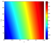
The intrinsic carrier concentration is given by [1]
where k is Boltzmann's constant, q is the elementary electric charge, t is the material temperature, x is the percentage of cadmium concentration, and Eg is the bandgap given by [2]


Using the relationship , where λ is in µm and Eg. is in electron volts, one can also obtain the cutoff wavelength as a function of x and t:
Minority carrier lifetime
Auger recombination
Two types of Auger recombination affect HgCdTe: Auger 1 and Auger 7 recombination. Auger 1 recombination involves two electrons and one hole, where an electron and a hole combine and the remaining electron receives energy equal to or greater than the band gap. Auger 7 recombination is similar to Auger 1, but involves one electron and two holes.
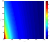
The Auger 1 minority carrier lifetime for intrinsic (undoped) HgCdTe is given by[3]
where FF is the overlap integral (approximately 0.221).
The Auger 1 minority carrier lifetime for doped HgCdTe is given by [4]
where n is the equilibrium electron concentration.
The Auger 7 minority carrier lifetime for intrinsic HgCdTe is approximately 10 times longer than the Auger 1 minority carrier lifetime:
The Auger 7 minority carrier lifetime for doped HgCdTe is given by
The total contribution of Auger 1 and Auger 7 recombination to the minority carrier lifetime is computed as
Mechanical
HgCdTe is a soft material due to the weak bonds Hg forms with tellurium. It is a softer material than any common III-V semiconductor. The Mohs hardness of HgTe is 1.9, CdTe is 2.9 and Hg0.5Cd0.5Te is 4. The hardness of lead salts is lower still.
Thermal
The thermal conductivity of HgCdTe is low; at low cadmium concentrations it is as low as 0.2 W·K−1m−1. This means that it is unsuitable for high power devices. Although infrared light-emitting diodes and lasers have been made in HgCdTe, they must be operated cold to be efficient. The specific heat capacity is 150 J·kg−1K−1.[5]
Optical
HgCdTe is transparent in the infrared at photon energies below the energy gap. The refractive index is high, reaching nearly 4 for HgCdTe with high Hg content.
Infrared detection
HgCdTe is the only common material that can detect infrared radiation in both of the accessible atmospheric windows. These are from 3 to 5 µm (the mid-wave infrared window, abbreviated MWIR) and from 8 to 12 µm (the long-wave window, LWIR). Detection in the MWIR and LWIR windows is obtained using 30% [(Hg0.7Cd0.3)Te] and 20% [(Hg0.8Cd0.2)Te] cadmium respectively. HgCdTe can also detect in the short wave infrared SWIR atmospheric windows of 2.2 to 2.4 µm and 1.5 to 1.8 µm.
HgCdTe is a common material in photodetectors of Fourier transform infrared spectrometers. It is also found in military field, remote sensing and infrared astronomy research. Military technology has depended on HgCdTe for night vision. In particular, the US air force makes extensive use of HgCdTe on all aircraft, and to equip airborne smart bombs. A variety of heat-seeking missiles are also equipped with HgCdTe detectors. HgCdTe detector arrays can also be found at most of the worlds major research telescopes including several satellites. Many HgCdTe detectors (such as Hawaii and NICMOS detectors) are named after the astronomical observatories or instruments for which they were originally developed.
The main limitation of LWIR HgCdTe-based detectors is that they need cooling to temperatures near that of liquid nitrogen (77K), to reduce noise due to thermally excited current carriers (see cooled infrared camera). MWIR HgCdTe cameras can be operated at temperatures accessible to thermoelectric coolers with a small performance penalty. Hence, HgCdTe detectors are relatively heavy compared to bolometers and require maintenance. On the other side, HgCdTe enjoys much higher speed of detection (frame rate) and is significantly more sensitive than some of its more economical competitors.
HgCdTe is often a material of choice for detectors in Fourier-transform infrared (FTIR) spectrometers. This is because of the large spectral range of HgCdTe detectors and also the high quantum efficiency.
HgCdTe can be used as a heterodyne detector, in which the interference between a local source and returned laser light is detected. In this case it can detect sources such as CO2 lasers. In heterodyne detection mode HgCdTe can be uncooled, although greater sensitivity is achieved by cooling. Photodiodes, photoconductors or photoelectromagnetic (PEM) modes can be used. A bandwidth well in excess of 1 GHz can be achieved with photodiode detectors.
The main competitors of HgCdTe are less sensitive Si-based bolometers (see uncooled infrared camera), InSb and photon-counting superconducting tunnel junction (STJ) arrays. Quantum well infrared photodetectors (QWIP), manufactured from III-V semiconductor materials such as GaAs and AlGaAs, are another possible alternative, although their theoretical performance limits are inferior to HgCdTe arrays at comparable temperatures and they require the use of complicated reflection/diffraction gratings to overcome certain polarization exclusion effects which impact array responsivity. In the future, the primary competitor to HgCdTe detectors may emerge in the form of Quantum Dot Infrared Photodetectors (QDIP), based on either a colloidal or type-II superlattice structure. Unique 3-D quantum confinement effects, combined with the unipolar (non-exciton based photoelectric behavior) nature of quantum dots could allow comparable performance to HgCdTe at significantly higher operating temperatures. Initial laboratory work has shown promising results in this regard and QDIPs may be one of the first significant nanotechnology products to emerge.
In HgCdTe, detection occurs when an infrared photon of sufficient energy kicks an electron from the valence band to the conduction band. Such an electron is collected by a suitable external readout integrated circuits (ROIC) and transformed into an electric signal. The physical mating of the HgCdTe detector array to the ROIC is often referred to as a "focal plane array".
In contrast, in a bolometer, light heats up a tiny piece of material. The temperature change of the bolometer results in a change in resistance which is measured and transformed into an electric signal.
Mercury zinc telluride has better chemical, thermal, and mechanical stability characteristics than HgCdTe. It has a steeper change of energy gap with mercury composition than HgCdTe, making compositional control harder.
HgCdTe growth techniques
Bulk crystal growth
The first large scale growth method was bulk recrystallization of a liquid melt. This was the main growth method from the late 1950s to the early 1970s.
Epitaxial growth
Highly pure and crystalline HgCdTe is fabricated by epitaxy on either CdTe or CdZnTe substrates. CdZnTe is a compound semiconductor, the lattice parameter of which can be exactly matched to that of HgCdTe. This eliminates most defects from the epilayer of HgCdTe. CdTe was developed as an alternative substrate in the '90s. It is not lattice-matched to HgCdTe, but is much cheaper, as it can be grown by epitaxy on silicon (Si) or germanium (Ge) substrates.
Liquid phase epitaxy (LPE), in which a substrate is repeatedly dipped into a liquid melt, gives the best results in terms of crystalline quality, and is still a common technique of choice for industrial production.
In recent years, molecular beam epitaxy (MBE) has become widespread because of its ability to stack up layers of different alloy composition. This allows simultaneous detection at several wavelengths. Furthermore, MBE, and also MOVPE, allow growth on large area substrates such as CdTe on Si or Ge, whereas LPE does not allow such substrates to be used.
Toxicity
The advancement of crystal growth technology has proceeded deliberately and steadily for four decades in spite of the high vapor pressure of Hg at the melting point of HgCdTe and the known [6] toxicity of the material.
See also
Related materials
Other infrared detection materials
- Indium antimonide, Indium arsenide, Lead selenide, QWIP, QDIP.
Other
References
- Notes
- ↑ Schmidt; Hansen (1983). "Calculation of intrinsic carrier concentration in HgCdTe". Journal of Applied Physics. 54. doi:10.1063/1.332153.
- ↑ Hansen (1982). "Energy gap versus alloy composition and temperature in HgCdTe". Journal of Applied Physics. 53. doi:10.1063/1.330018.
- ↑ Kinch (2005). "Minority Carrier Lifetime in p-HgCdTe". Journal of Electronic Materials. 34.
- ↑ Redfern (2001). "Diffusion Length Measurements in p-HgCdTe Using Laser Beam Induced Current". Journal of Electronic Materials. 30.
- ↑ Chen, C S; Liu, A H; Sun, G; He, J L; Wei, X Q; Liu, M; Zhang, Z G; Man, B Y (2006). "Analysis of laser damage threshold and morphological changes at the surface of a HgCdTe crystal". Journal of Optics A: Pure and Applied Optics. 8: 88. doi:10.1088/1464-4258/8/1/014.
- ↑ http://www.arl.army.mil/arlreports/2009/ARL-TR-5033.pdf
- Bibliography
- Preparation and properties of HgTe and mixed crystals of HgTe-CdTe, W. D. Lawson, S. Nielson, E. H. Putley, and A. S. Young, J. Phys. Chem. Solids vol. 9, 325–329 (1959). (Earliest known reference)
- Properties of Narrow-Gap Cadmium-Based Compounds, Ed. P. Capper (INSPEC, IEE, London, UK, 1994) ISBN 0-85296-880-9
- HgCdTe Infrared Detectors, P. Norton, Opto-Electronics Review vol. 10(3), 159–174 (2002)
- Rogalski, A (2005). "HgCdTe infrared detector material: history, status and outlook". Reports on Progress in Physics. 68 (10): 2267. doi:10.1088/0034-4885/68/10/R01.
- Chen, A B; Lai-Hsu, Y M; Krishnamurthy, S; Berding, M A (1990). "Band structures of HgCdTe and HgZnTe alloys and superlattices". Semiconductor Science and Technology. 5 (3S): S100. doi:10.1088/0268-1242/5/3S/021.
- E. Finkman and Y. Nemirovsky, J. Appl. Phys. 50, 4356 (1979).
- Finkman, E.; Schacham, S. E. (1984). "The exponential optical absorption band tail of Hg1−xCdxTe". Journal of Applied Physics. 56 (10): 2896. doi:10.1063/1.333828.
- Bowen, Gavin J. (2005). "HOTEYE: a novel thermal camera using higher operating temperature infrared detectors". 5783: 392. doi:10.1117/12.603305..
- Semiconductor Quantum Wells and Superlattices for Long-Wavelength Infrared Detectors M.O. Manasreh, Editor (Artech House, Norwood, MA), ISBN 0-89006-603-5 (1993).